πŸ”¬ FLUXMATERIA — MATERIALS

Work function, band alignment,
and contact design in one studio

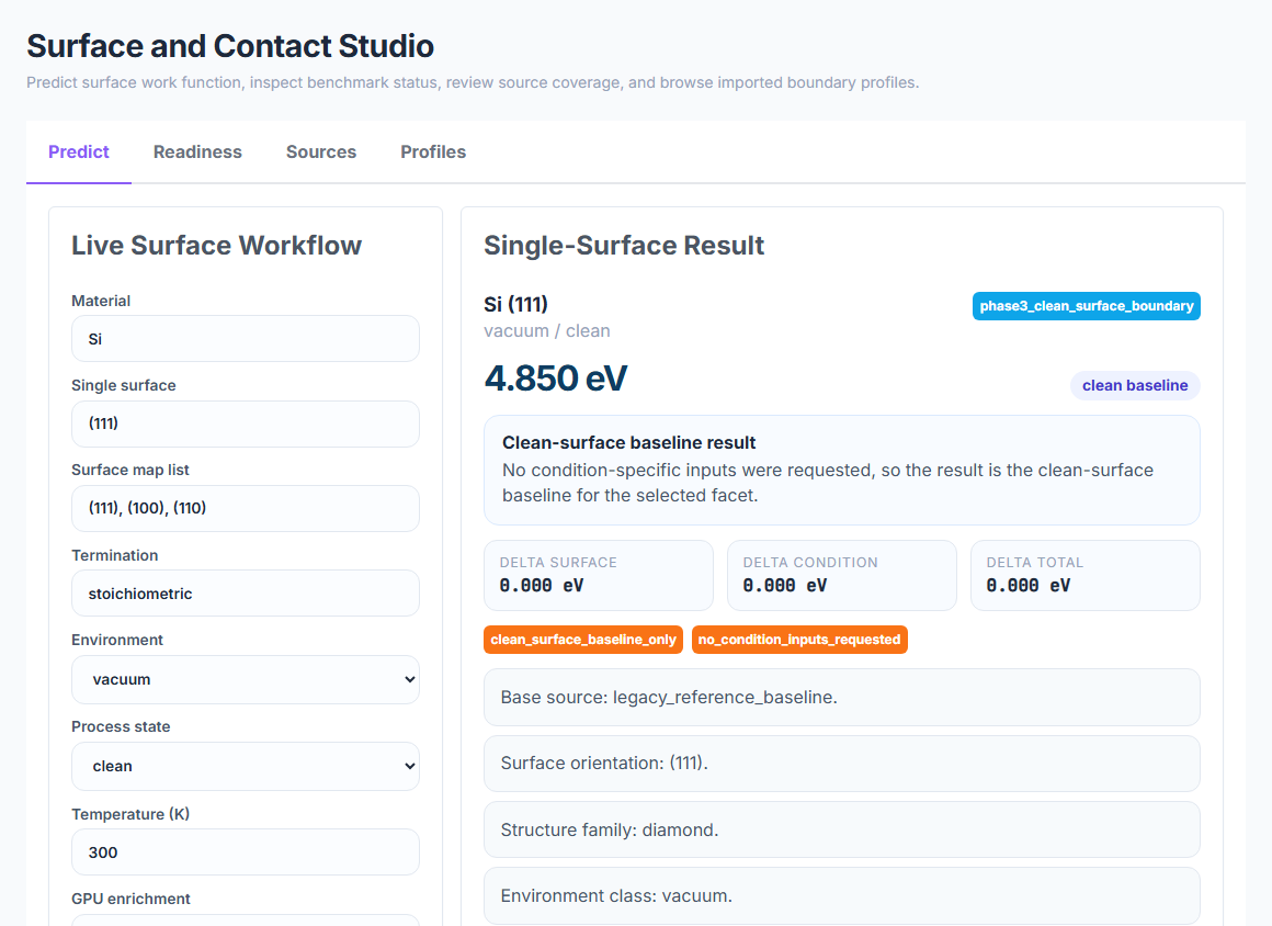
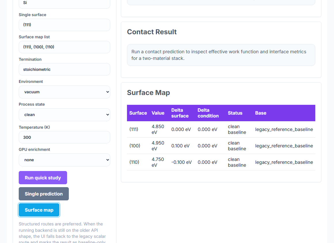
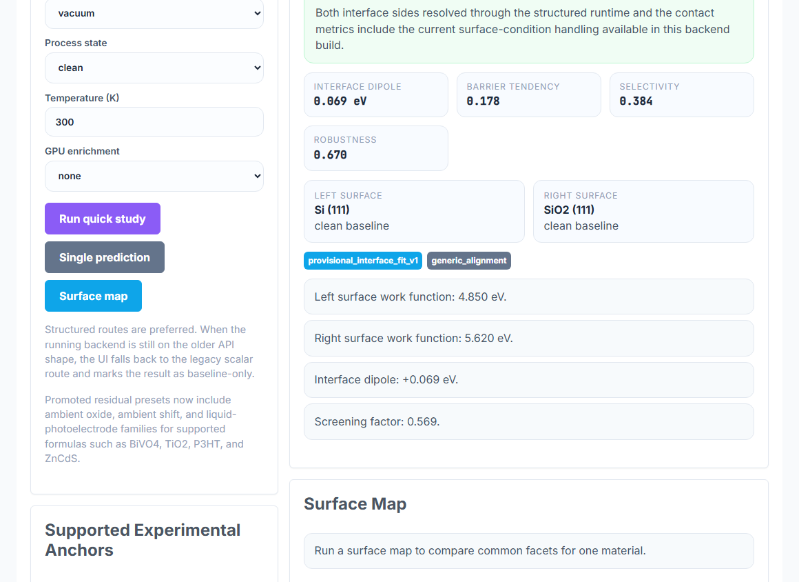
Predict the clean-surface work function for any material and facet, sweep work functions across a facet map, and engineer any contact — effective work function, band alignment, Schottky barrier — with environment and process state as first-class inputs.

Clean-surface work function Facet map Schottky barrier Environment & process Open-source validation
0.063 eV
MAE across 35 experimental interface stacks (100% pass@0.25 eV)
0.059 eV
MAE on the 6-stack curated interface set (100% pass@0.25 eV)
193
Experimental surface records across 77 materials
17
Open-source datasets (Zenodo) backing the validation
0
Trained parameters
The breakthrough

A surface prediction that remembers the sample was in air

Work function and Schottky barrier depend on the surface as much as on the bulk. This module takes the material and the facet, yes — and the environment (vacuum, ambient, humid), the process state (annealed, ion-sputtered, lithiated, illuminated), and the temperature. The returned value is the condition-dependent surface work function, with every applied correction reported alongside it and traced back to the published dataset it came from.

What Surface & Contact does

Three live prediction workflows, backed by a catalog of approved experimental sources.

🧭

Clean-surface work function

Material + Miller-index facet + termination + environment + process + temperature → condition-dependent work function with every applied delta broken out.

πŸ—ΊοΈ

Surface map (facet sweep)

Sweep multiple facets of the same material in one request. Pristine vs Ti-doped MoS2, (100)/(110)/(111) of an FCC metal — one table.

πŸ”—

Interface & Schottky barrier

Pair any two materials with chosen surfaces and terminations. Returns effective work function, band alignment, interface dipole, Schottky barrier height.

🌫️

Environment & process aware

Vacuum, ambient, dry air, humid air, liquid photoelectrode; annealed, ion-sputtered, lithiated, illuminated — 20+ process states are first-class inputs.

πŸ“Š

Readiness dashboard

Dashboard surfaces benchmark status (stable / watch), blockers, featured sources, and the Readiness Catalog with data staging tier per source.

πŸ“œ

Source evidence

Click any source to see extraction method (UPS / XPS secondary-electron cutoff), baseline-fit R2, uncertainty, and the Zenodo archive member.

🧩

Stack family catalog

Perovskite-on-TMO, oxide-on-oxide, and other stack families carry curated priors and dedicated alignment models.

πŸ”

Interface batch

Multiple interface stacks in one request with CSV-friendly rows — sweep contact pairs for a device design space.

How a surface / contact prediction is built

From material and facet to a condition-dependent result in one call.

1

Configure

Material formula, Miller-index facet, termination, environment, process state, temperature — and, for contacts, the right-hand-side material and contact geometry.

2

Bulk anchor

Universal materials engine supplies bulk work function, band gap, dielectric, and density — the baseline the surface model sits on top of.

3

Surface layer

Clean-surface prediction for the chosen facet + termination, with experimental priors applied where the observed family matches.

4

Condition delta

Environment and process state apply their own residual models — ambient oxide, humidity, light, ion-sputter — each reported as a separate component.

5

Return

Work function (eV), applied-component breakdown, runtime mode (clean baseline vs observed prior vs thin-film prior vs family residual), calibration version.

Why you can trust it

Validation against 193 surface records and 35 interface stacks, all from open datasets.

0.063 eV
MAE on 35 experimental interface stacks — 100% pass-rate at the 0.25 eV threshold.
0.059 eV
MAE on the 6-stack curated interface set — 100% pass-rate at 0.25 eV.
0.258 eV
MAE on the 17-record oxide contextual-surface set (live “watch” benchmark).
193
Experimental surface records across 77 materials (UPS / XPS secondary-electron cutoff).
17
Open-source datasets feeding validation (Zenodo: InP PES, MoS2 KPM / SECCM, Cu2O, NiO, perovskite interlayer stacks).
0
Trained parameters. Every prediction is deterministic and re-runnable.

How FluxMateria compares

Head-to-head against the common sources of work function and Schottky-barrier numbers.

MetricFluxMateriaMichaelson handbookDFT slab calcSchottky-Mott rule
Interface MAE (eV)0.063Not applicable0.2–0.50.5–1.5
Environment-awareYes, 6+ classesVacuum onlyVacuum onlyVacuum only
Process state-aware20+ statesNoneUsually noneNone
Latency per predictionSub-secondInstant lookupHours to daysInstant
Predicts new materialsYesNoYes (slow)Yes (inaccurate)
Facet sweep in one callYesNoOne slab per facetNo
Data provenance per resultSource + archive + R2Handbook entryMethod traceRule only
Condition-delta breakdownEvery component reportedNoneNoneNone

The key insight: Handbook work functions are exact but vacuum-only; DFT slab calculations cover the bulk but cost hours per facet; the Schottky-Mott rule is a back-of-envelope estimate with ~1 eV error bars. Surface & Contact wraps a first-principles engine with curated experimental priors and environment / process deltas, so the number you ship already accounts for how the sample was made and measured. See the materials benchmark →

Where Surface & Contact wins

Engineering workflows where the sample history is the prediction.

Use case 1

Device contact design

Pick an FET channel and two contact metals, sweep facets, read Schottky barrier and band alignment for each. Pick the pair that actually makes ohmic contact.

Use case 2

Solar interlayer selection

Perovskite-on-TMO stacks with curated priors. Effective work function and interface dipole for each interlayer choice, before depositing a sample.

Use case 3

Photoelectrode design

BiVO4, Cu2O, TiO2 under ambient or liquid conditions. The environment class shifts the work function in the direction the experiment would.

Use case 4

Process-sensitivity audit

Compare as-deposited vs annealed vs ion-sputtered for the same material. See which process state matches the lab’s actual measurement.

Use case 5

Literature cross-check

A paper reports 4.7 eV for Cu(111) ambient. Check the prediction, the applied delta, and the Zenodo source it was calibrated against.

Use case 6

Compliance & audit

Every number carries its runtime mode, applied components, and calibration version. Reproducible, auditable, and traceable back to the open data.

Surface & Contact in the product

Real captures from the live application. Click any image to zoom.

Surface prediction panel with material, facet, environment, process state, and work function result
Clean-surface predictionMaterial, facet, environment, process → work function and the applied-component breakdown.
Surface map table sweeping multiple facets of the same material
Surface mapMulti-facet sweep for one material — each row carries work function, baseline, and applied deltas.
Interface prediction with pair selection and Schottky barrier result
Interface & Schottky barrierPair any two materials, pick surfaces and contact geometry, read the effective work function and barrier.
Readiness dashboard with benchmark status, blockers, source catalog, and validation coverage
Readiness dashboardBenchmark status per series, blockers, featured sources, and validation coverage across families.

Scope & Limitations

Strengths

  • 0.063 eV MAE and 100% pass-rate at 0.25 eV on 35 experimental interface stacks.
  • Environment and process state are first-class inputs, not after-the-fact corrections.
  • Every result carries its applied-component breakdown, runtime mode, and the dataset it was calibrated against.
  • Facet map and interface batch let you sweep design space in one call, CSV-ready.
  • All validation data comes from open-source Zenodo datasets — no proprietary calibration.

Known limitations

  • The oxide contextual-surface benchmark is currently in “watch” status (0.26 eV MAE); the interface path is stable.
  • Covers inorganic surfaces and interfaces; organic semiconductor surfaces are scheduled for a later release.
  • For doped-junction device simulation (drift mobility, FoMs), use the Semiconductor Design module.
  • Rare stack families without experimental priors fall back to a general alignment model with wider error bars.

Design the contact your device actually has

Pilot access includes the Surface & Contact studio, the readiness dashboard, interface batch, and a Workspace seat to keep every prediction auditable.

Request Pilot Access →