πŸ’  FLUXMATERIA — MATERIALS

Mobility across the full design space.
In milliseconds.

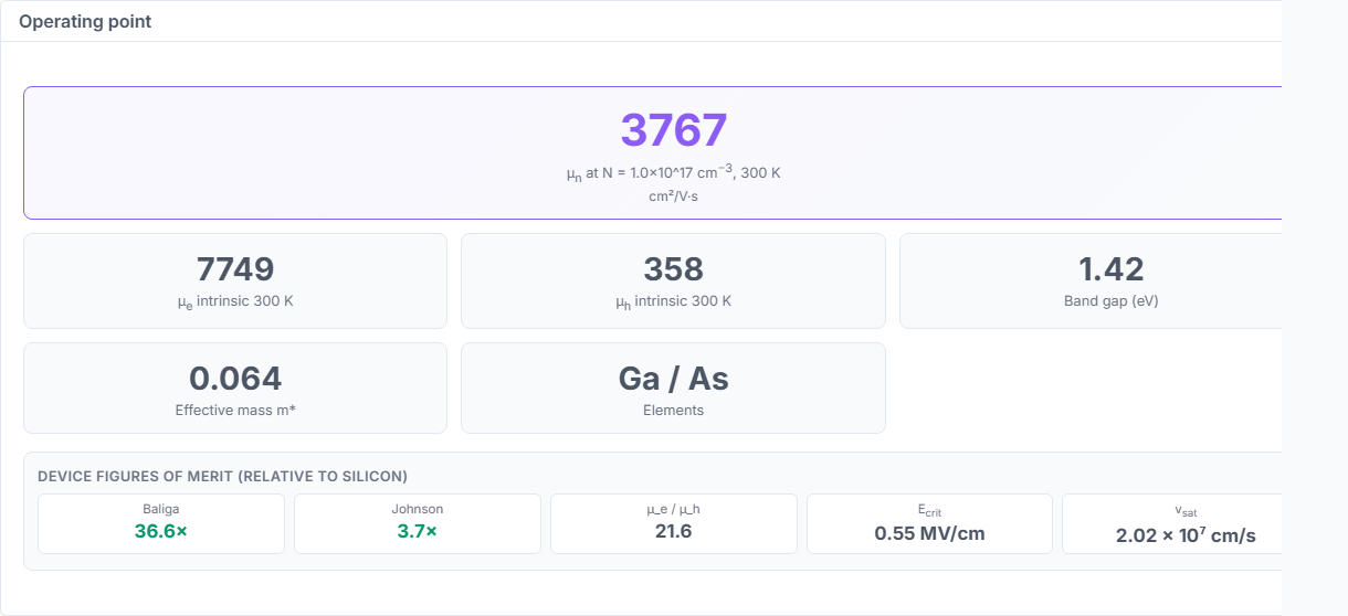
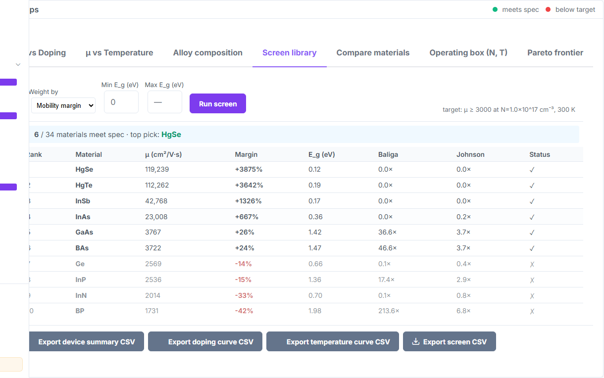
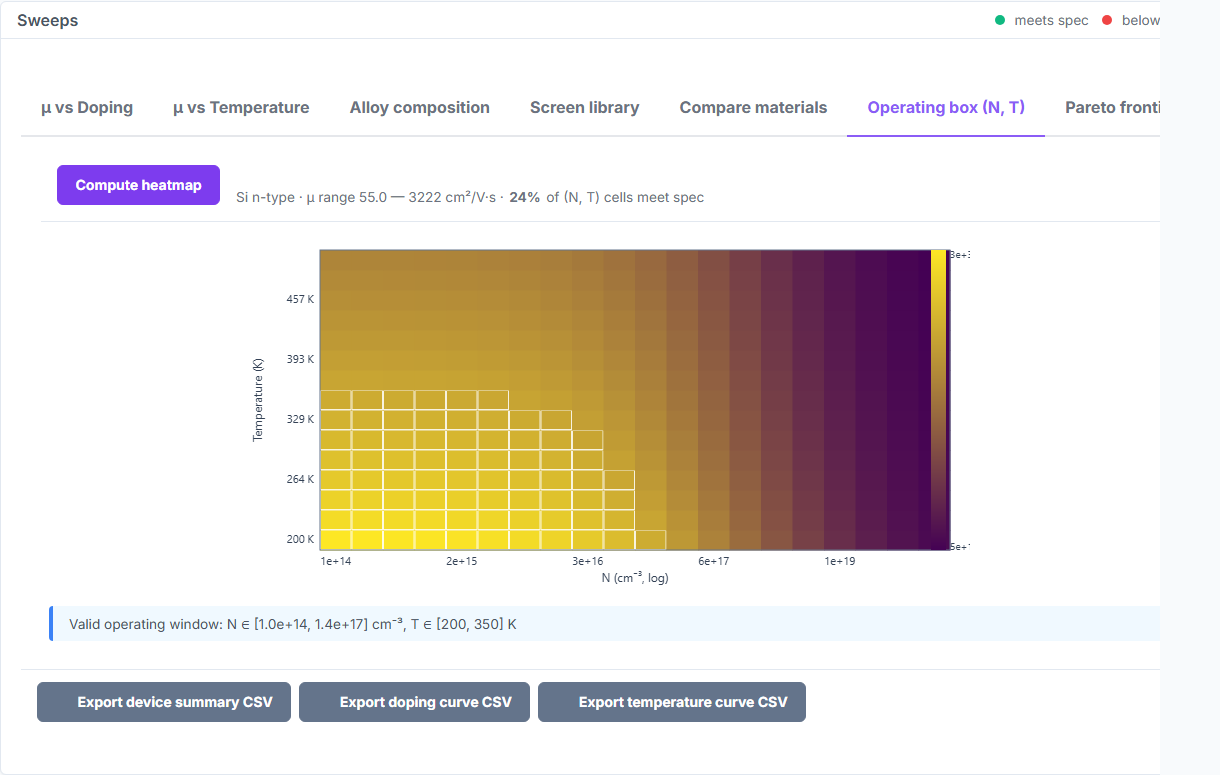
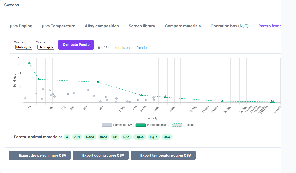
Drift-mobility prediction across material family, doping concentration, temperature, and ternary alloy composition — with device targets, inverse spec search, (N, T) operating heatmaps, Pareto frontiers, and CSV export. First-principles physics, zero fitted parameters.

22 preset materials 34-material screening library 5 figures of merit Sub-millisecond evaluation CSV export
6.2%
μe intrinsic MAPE on 26 semiconductors
4.4%
μh intrinsic MAPE on 30 reliable materials
15.9%
Doping-curve MAPE across 5 decades of N
7.6%
InGaAs alloy MAPE incl. lattice-matched x=0.47
0
Fitted parameters · 0 training data
The breakthrough

The mobility design space is continuous. The tool should be too.

Mobility tables give you a point. First-principles BTE solvers give you a weekend per material. Semiconductor Design gives you the full continuous surface — across 34 materials, 5 decades of doping, 77–500 K, and alloy composition — in under a millisecond per evaluation. Every point is a calculation, not an interpolation. Every point carries the same 6.2% MAPE band as the benchmarks.

What the module gives you

Eight design capabilities, one continuous surface.

πŸ“ˆ

Live mobility across doping

Drift mobility computed across 5 decades of dopant concentration, per material, per carrier type — update the sliders and the curve redraws.

🌑️

Temperature sweep 77–500 K

Full T-dependence from liquid-nitrogen to power-device operating windows. Phonon-limited and ionized-impurity regimes resolved in the same pass.

🎯

Design targets with pass/fail

Set target thresholds on mobility, breakdown field, band gap, and figures of merit. Every candidate renders a green / red gate instantly.

πŸ”Ž

Inverse spec search

“Find me a material with μe ≥ 3000 at T = 300 K.” The engine ranks the 34-material library by mobility margin, Baliga FoM, Johnson FoM, or balanced score.

πŸ“Š

Material comparison overlay

Overlay mobility curves for up to six materials on the same axes. Read the crossover points where ranking flips with temperature or doping.

πŸ—ΊοΈ

(N, T) operating-box heatmap

2D heatmap of mobility across dopant concentration and temperature. Draw the feasibility box that satisfies your device spec.

πŸ†

Pareto frontier

Plot any two of mobility / band gap / breakdown field / Johnson FoM / Baliga FoM. Pareto-optimal materials flagged; dashed line traces the frontier.

πŸ“€

CSV export

Every surface, curve, and Pareto candidate exportable as CSV — ready for the device-simulation handoff or a publication supplementary.

A 60-second discovery loop

From “what material do I need?” to a ranked shortlist with operating bounds.

1

Set the spec

Mobility floor, band-gap window, breakdown field, device target. Pick the figure of merit that matches your use case.

2

Sweep materials

Run the inverse search across the 34-material library. Every candidate evaluated at your (T, N) point in sub-ms.

3

Tune the knobs

Adjust doping, temperature, and alloy composition. Curves redraw live; pass/fail gates update in place.

4

Box the operating window

(N, T) heatmap + feasibility contour. See exactly which dopant / temperature combinations clear the spec.

5

Check the frontier

Pareto plot across two figures of merit — identify the trade-offs the single-number ranking was hiding.

6

Export

CSV of ranked candidates, their operating bounds, and their pass/fail decisions — ready for the device team.

Why you can trust it

Calibrated against 30+ semiconductors, 5 decades of doping, and real ternary alloys.

6.2%
μe intrinsic MAPE on 26 semiconductors. In the accuracy band of first-principles BTE solvers, at millisecond cost.
4.4%
μh intrinsic MAPE on 30 reliable materials. Holes are usually the hard case; here the model is tighter than the electrons.
15.9%
Doping-curve MAPE across 5 decades of N. Phonon, ionized-impurity, and alloy scattering regimes all covered in one pass.
7.6%
InGaAs alloy MAPE including the lattice-matched x=0.47 composition — the industrial reference point.
34
Materials in the screening library covering III-V, II-VI, IV-IV, oxides, and wide-gap power-device channels.
0
Fitted parameters. 0 training data. Same input → same ranking, bit-for-bit, every run.

How FluxMateria compares

Mobility tables vs BTE solvers vs a continuous design surface.

CapabilityFluxMateriaPublished mobility tablesFirst-principles BTE (EPW, Perturbo)ML surrogates
Electron MAPE6.2% (26 mat)Reference (point)5–15%10–20%
Hole MAPE4.4% (30 mat)Reference (point)10–25%15–25%
Time per evaluationSub-msInstant lookupCPU-days per materialSeconds
Doping sweep5 decades, continuousFew discrete pointsWeeks per curveInterpolated
Temperature sweep77–500 K liveRoom T mostlyOne temperature at a timeInterpolated
Alloy compositionContinuousDiscrete endpointsExpensive per xOften excluded
Inverse spec searchBuilt-inManualNot practicalRare
Training dataNoneExperimentalNoneThousands of BTE runs

The key insight: Mobility tables give you a point. BTE solvers give you a calculation per material, per week. FluxMateria gives you the full continuous surface across material, doping, T, and alloy composition in under a millisecond per evaluation — with the same MAPE band as published BTE numbers. See the full benchmark →

Where Semiconductor Design wins

Device-design loops where the question is the window, not a single material.

Use case 1

Power-device channel selection

Wide-gap channel materials ranked by Baliga FoM at your operating temperature. Operating-box heatmap bounds the safe (N, T) window.

Use case 2

RF design

Johnson-FoM Pareto frontier across compound semiconductors — find the mobility / breakdown trade-off that wins your node.

Use case 3

Alloy optimization

Sweep InGaAs / AlGaAs / SiGe composition continuously. Find the x that maximizes mobility at your lattice-matching constraint.

Use case 4

Doping targeting

Find the dopant concentration window that maximizes mobility given your threshold-voltage or contact-resistance spec.

Use case 5

Cryogenic design

77–150 K mobility behaviour for superconducting-adjacent electronics and quantum-compute channel materials.

Use case 6

Supply-chain substitution

“What non-GaAs III-V hits my mobility floor?” Inverse search returns the alternatives that clear the spec within one click.

Semiconductor Design in the product

Real captures from the live application. Click any image to zoom.

Live mobility evaluation at a single operating point
Live operating pointMobility, breakdown field, and figures of merit at a single (material, N, T, x) point — updates in real time as the sliders move.
Inverse spec search with ranked candidates
Ranked shortlistInverse spec search across the 34-material library — candidates ranked by mobility margin, Baliga, Johnson, or balanced score.
(N, T) operating-box mobility heatmap
Operating-box heatmapMobility across dopant concentration and temperature. Draw the feasibility box that satisfies the device spec.
Pareto frontier across two figures of merit
Pareto frontierAny-two-FoM plot with Pareto-optimal materials flagged and the frontier traced — the trade-offs single-number ranking hides.

Scope & Limitations

Strengths

  • 6.2% electron / 4.4% hole MAPE on 30+ semiconductors — in the BTE accuracy band, at sub-ms cost.
  • Continuous surface across material, doping (5 decades), temperature (77–500 K), and alloy composition.
  • Inverse spec search + Pareto frontier + operating-box heatmap — design loops measured in seconds.
  • Zero fitted parameters, zero training data. Every surface point is a calculation, not an interpolation.
  • 34-material screening library covers III-V, II-VI, IV-IV, oxides, and wide-gap power-device channels.

Known limitations

  • Library is 34 materials today; custom compositions require a pilot workshop to add to the screening set.
  • Scattering physics targets phonon + ionized-impurity + alloy regimes; deep-level-trap-limited mobility requires explicit defect input.
  • 2D-material and heterostructure mobility (quantum-confined channels) is on the roadmap but not in v1.
  • Device-level simulation (drain current, BV, Ron) lives in partner tools; Semiconductor Design hands off material-level inputs with operating bounds.

Design semiconductors in the space they actually live in.

Pilot access includes Semiconductor Design, the universal Materials engine, Battery Electrochemistry, Surface & Contact, and a Workspace seat for audit-ready runs.

Request Pilot Access →